User Manual
Task-oriented documentation for ZofzPCB. New to ZofzPCB? Start with the Quick-start Guide to get your first board loaded in minutes.
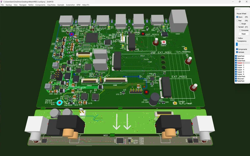
Loading your project
Eight articles covering every way to get your design files into ZofzPCB.
Feature overview →1.1 Auto Load (Gerber set)
The fastest way to load a Gerber project. ZofzPCB scans your folder, identifies your files, and proposes the stackup automatically.
When to use this
You have a folder containing your Gerber files (copper layers, drill files, board outline) and want to get into the 3D view as quickly as possible.
Steps
- Go to File → Auto Load (Gerber Set)
- Select the folder containing your Gerber files
- ZofzPCB scans the folder and displays the detected files with their proposed layer assignments
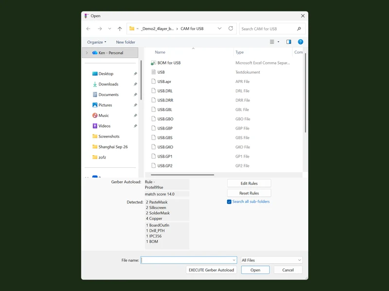
- Review the assignments: confirm that top copper, bottom copper, drill files, and board outline are correctly identified
- If any file is misidentified, right-click its row and select Remove or reassign it manually
- Press Execute Auto Load
- The stackup dialog opens: review and complete the stackup parameters before proceeding
- Press OK: Read & Render
How the autoloader works
ZofzPCB identifies files by matching their names and extensions against a set of naming rules stored in %APPDATA%\ZofzPCB\CAM_Load_Rules.txt. This file contains rules for common CAD tool conventions including KiCad, Eagle, Altium, and Protel. If your files use non-standard naming, the autoloader may not detect all layers correctly: use Manual Compose instead.
1.2 Manual Compose (Gerber set)
Full manual control over file assignment and layer order. Use this when Auto Load does not correctly identify your files.
When to use this
Auto Load produced incorrect or incomplete layer assignments, or your project uses a non-standard naming convention.
Steps
- Go to File → New (For Manual Compose)
- A Stackup dialog and a File Explorer window open side by side
- Drag and drop your Gerber files from the File Explorer into the correct slots in the Stackup dialog
- To add core or pre-preg dielectric layers, right-click the Name column and select Add Uniform Layer
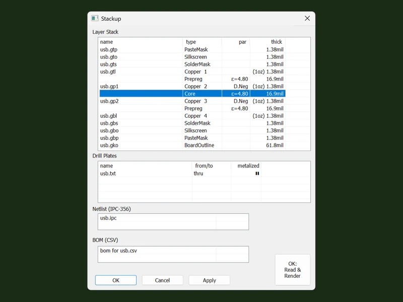
- Arrange layers in the correct order (top to bottom, component side to solder side) by dragging rows up and down
- Assign drill plate parameters: specify start and end copper layers and set the via type
- Check the polarity of each layer: solder mask and paste are typically negative; copper is typically positive
- Press OK: Read & Render
Stackup dialog columns
| Column | Description |
|---|---|
| Name | Filename if a Gerber file is assigned to this layer |
| Type | Layer type: copper, solder mask, silkscreen, core, pre-preg etc. |
| Par | Additional parameters: polarity, special settings |
| Thick | Layer thickness. For copper, enter in oz (oz per square foot) |
Drill plate via types
| Type | Description |
|---|---|
| Non-plated | Plain, non-conductive hole |
| Plated | Conductive barrel: standard through-hole |
| Filed | Conductive barrel, metal filled or capped |
| µVia↓ | Blind via: metalized from bottom |
| µVia↑ | Blind via: metalized from top |
| µVia↓ Filed | Blind via, filled, metalized from bottom |
| µVia↑ Filed | Blind via, filled, metalized from top |
1.3 Loading ODB++
ODB++ loads as a single file, no stackup configuration needed.
When to use this
Your CAD tool exports ODB++ format. ODB++ is a self-contained format that includes layer data, netlist, component information, and stackup in a single file or compressed folder.
Steps
- Go to File → Open
- Navigate to your ODB++ file and select it
- ZofzPCB reads the file and builds the board automatically, no manual layer assignment required
- The stackup dialog opens for review: ODB++ includes stackup information so most parameters will be pre-filled
- Confirm the stackup and press OK: Read & Render
.gz compression. ZofzPCB reads them directly: you do not need to extract them first.1.4 Loading IPC-2581
IPC-2581 is a single XML file containing everything ZofzPCB needs, including stackup, netlist, and component data.
When to use this
Your CAD tool exports IPC-2581 format. It is the most complete single-file format supported by ZofzPCB: layer data, stackup, netlist, BOM, and component information in one structured file.
Steps
- Go to File → Open
- Navigate to your IPC-2581 file (
.xml) and select it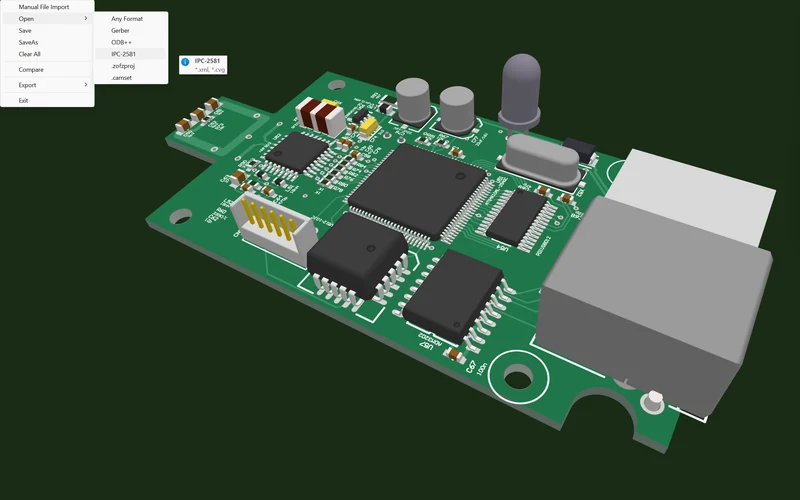
- ZofzPCB reads the file and builds the board automatically
- The stackup dialog opens for review: all parameters should be pre-filled
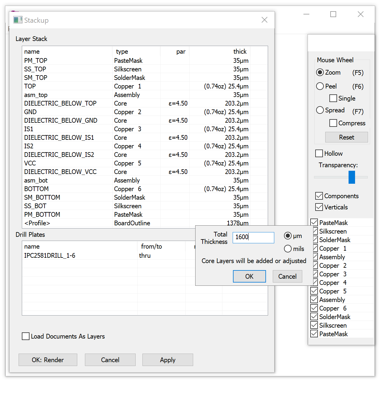
- Confirm and press OK: Read & Render
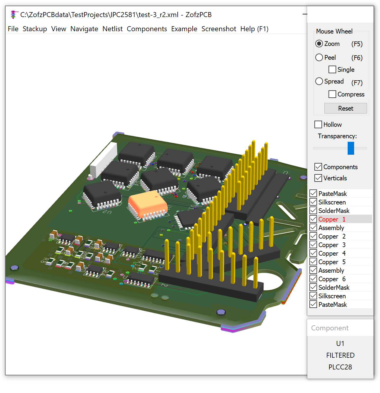
Why IPC-2581 is the recommended format
Because IPC-2581 carries complete design information in a single file, loading is simpler and the 3D model is typically more accurate than a Gerber set. If your CAD tool supports it, use it.
1.5 Loading from ZIP
ZofzPCB can read Gerber sets, .camset files, and IPC-2581 files directly from ZIP archives without extracting them first.
When to use this
Your design files are delivered or stored as a ZIP archive.
What works with ZIP
| Format | ZIP supported? |
|---|---|
| Gerber file set | Yes. Treated as a folder |
| .camset configuration file | Yes. Read and save |
| IPC-2581 | Yes. Extracted automatically |
| .zofzproj rendered project | No. Uses its own LZMA compression |
| ODB++ | No. May use its own gz compression |
Steps
- Go to File → Auto Load or File → Open as normal
- Navigate to the ZIP file: ZofzPCB displays the ZIP contents as if it were a folder
- Proceed with loading as normal
1.6 Custom autoload rules
Autoload recognizes files by their names. If your CAD tool uses names ZofzPCB doesn't know, add your own rules:
- Click
Edit Rulesin the autoload panel. This opensCAM_Load_Rules.txt(in%APPDATA%\ZofzPCB); the file explains its format at the top. - Write file masks in lowercase.
- Masks can include a folder, e.g.
Drill_PTH *\*.drlfor drill files in a subfolder. - Examples from users, Altium:
Drill_PTH *_pth_drill.gbr,Drill_NPTH *_npth_drill.gbr,BoardOutline *_profile.gbr. P-CAD:.tps/.bpspaste,.gto/.gbosilkscreen,.tms/.bmssolder mask,.top/.bot/.inNcopper,.gkooutline,.ncdplated drills. - Updates keep your rules.
Reset Ruleson the Gerber Load dialog restores the rules that ship with ZofzPCB.
1.7 Auto-Offset and the Drill / Pad Fit Warning
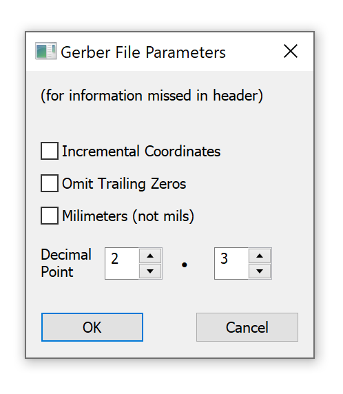
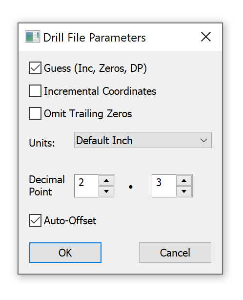
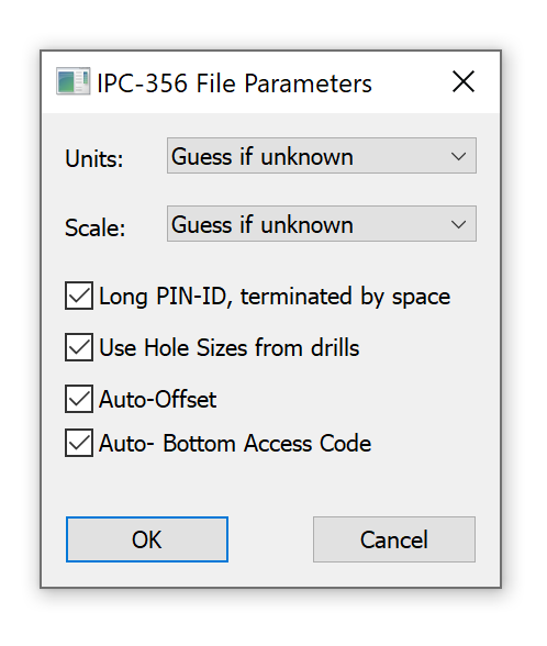
Gerber and drill files are often exported with different offsets, so ZofzPCB shifts the drill data onto the pads automatically (Auto-Offset, on by default). The Drill / Pad Fit Warning means only a few drill holes matched pads. If your files are exported correctly, turn Auto-Offset off: right-click Drill Plates, Setup Excellon Format.
1.8 Panel outlines
ZofzPCB builds the board shape from the board outline layer. For a panel, set how the outline is interpreted in the Board Outline setup; ZofzPCB remembers the setting. Closed shapes on the outline layer, such as the letters “P” or “0”, create extra outlines, so keep text off that layer.
Configuring the stackup
Seven articles covering stackup setup: the critical step between loading your files and rendering your board.
Feature overview →2.1 Reviewing the stackup
Before ZofzPCB renders your board it proposes a stackup. This is your moment to review and complete it.
When to use this
Every time you load a Gerber set, before pressing Read & Render.
What to check
- Layer order: top copper at the top, bottom copper at the bottom, inner layers in correct sequence
- All copper layers present: count them against your CAD tool's layer stack
- Board outline identified: the PCB boundary layer must be assigned
- Drill files linked: each drill file assigned to the correct copper layer span
- Dielectric layers present: core and pre-preg between each copper layer
2.2 Layer types and thickness
Gerber files carry copper artwork but not stackup parameters. Enter these manually for accurate DFM validation.
When to use this
After loading a Gerber set, when you want full stackup parameters for DFM validation or accurate STEP export.
Parameters to enter
| Parameter | Description |
|---|---|
| Layer type | Core or pre-preg for dielectric layers |
| Thickness | Layer thickness in millimetres |
| Copper weight | Typically 1oz, 2oz, or 0.5oz per copper layer |
| Material | FR4, Rogers, polyimide, or other substrate |
Steps
- Open the Stackup dialog (Stackup → Display/Edit)
- For each dielectric layer, click the Type column and select Core or Pre-preg
- Click the Thick column and enter the thickness in mm
- For copper layers, enter the copper weight using oz notation (e.g.
1oz) - Enter the total PCB thickness in the Board Outline thickness field: ZofzPCB adjusts the core/pre-preg layers to match
2.3 Drill plates and via types
Configure drill files to correctly represent through-holes, blind vias, buried vias, and µVias.
When to use this
When your board uses multiple drill files, non-standard via types, or blind and buried vias.
Drill plate columns
| Column | Description |
|---|---|
| Name | Filename of the drill file |
| From/To | Start and end copper layer numbers |
| Type | Via type: see table below |
Via types
| Type | Description |
|---|---|
| Non-plated | Plain, non-conductive hole |
| Plated | Conductive barrel: standard through-hole |
| Filed | Conductive barrel, metal filled or capped |
| µVia↓ | Blind via: metalized from bottom |
| µVia↑ | Blind via: metalized from top |
| µVia↓ Filed | Blind via, filled, metalized from bottom |
| µVia↑ Filed | Blind via, filled, metalized from top |
Steps
- In the Stackup dialog, locate the Drill Plates section
- Set From and To columns to the copper layers the drill spans
- Set the Type column to the correct via type
- If a drill file contains both holes and routing, add both to the Drill Plates list
2.4 Board outline
The board outline defines the physical boundary of the PCB. ZofzPCB needs it to correctly render and clip the board.
Methods ZofzPCB supports
- Standard outline layer: a dedicated Gerber layer for the board boundary (most common). Detected automatically in Auto Load.
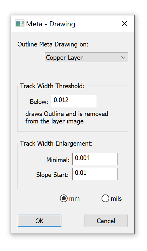
- Meta drawing: the outline is drawn on a copper or silkscreen layer using thin tracks. Set a thickness threshold via right-click on the layer in the Stackup dialog.
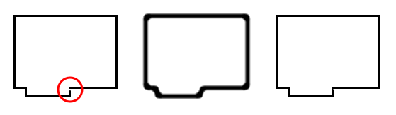
- Identify outline: for M2M files where the outline must be inferred:
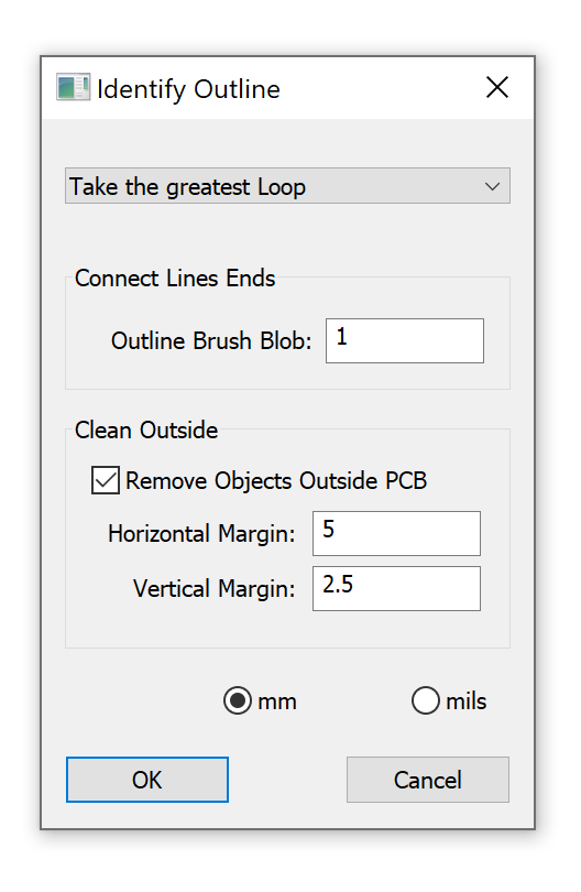
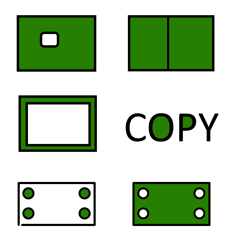
| Option | Description |
|---|---|
| Accept all detected loops | All detected outlines define multiple PCBs |
| Auto recognition | Finds a division line between the PCB and drawing text |
| Take the greatest loop | Assumes the largest shape is the PCB |
| Take 2–10 greatest loops | For boards with multiple outlines or cutouts |
Steps (standard)
- In the Stackup dialog, confirm the Board Outline layer is assigned to the correct Gerber file
- Enter the total PCB thickness in the Board Outline Thick field
2.5 Saving your stackup (.camset)
Save your stackup configuration so you don't have to re-enter settings when you regenerate Gerber files.
What .camset saves
Layer assignments and order · Layer types, thicknesses, and materials · Drill plate assignments · IPC-356 and BOM filenames · Colour settings · Gerber/drill/IPC-356 file format parameters · Board outline settings · Camera positions · Component model adjustments and Body Builder models
To save
- Go to File → Save As
- In the Save As Type dropdown, select .camset
- Choose a filename and location: keep it in the same folder as your Gerber files
- Press Save
To load
- Go to File → Open and select the .camset file
- ZofzPCB re-reads the Gerber files using the saved settings
- Or double-click the .camset file directly
2.6 Saving your project (.zofzproj)
Save the complete rendered board, including all component models and settings, as a single project file.
Difference between .camset and .zofzproj
| .camset | .zofzproj | |
|---|---|---|
| Saves rendered board | No | Yes |
| Saves configuration | Yes | Yes |
| File size | Small | Larger |
| Use case | Re-load after Gerber regeneration | Save complete session |
To save
- Go to File → Save As
- Select .zofzproj in the Save As Type dropdown
- Choose a filename and press Save
To save as view-only (free)
- In the Save As dialog, check the View-Only Mode option before saving
- The file can be opened by anyone in the free version: they can view but not modify or export
2.7 Blind and buried via spans
Each drill plate has a from/to span. Right-click the from/to column to set it: top (copper 1), btm (last copper), thru (top to bottom) or the copper numbers of an inner span. Autoload can read the span from the file name: a mask like *_*_drill_N_N.gbr uses the two numbers as the from and to copper layers.
Viewing in 3D
Ten articles covering navigation, layer control, cross-sections, and rendering options.
Feature overview →3.2 Layer panel and toggles
Turn individual layers on and off to focus on what matters.
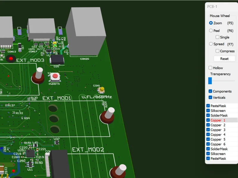
The right panel
The right panel contains checkboxes for every layer in your stackup, plus:
- Components: toggle 3D component models on/off
- Verticals: toggle via barrels and pads on/off
- Transparency slider: make all layers semi-transparent
- Hollow: render the board as a hollow shell
Steps
- The right panel is visible by default on the right side of the screen
- Click any layer checkbox to hide or show it
- Use the Components checkbox to toggle all component models at once
- Drag the Transparency slider to make layers semi-transparent
3.3 Peel and expand layers
Separate the layers of your board to inspect the stackup from the inside.
Peel
Removes layers from the top down, like peeling back the board one layer at a time.
- Press F6 to peel the top layer
- Press repeatedly to peel multiple layers
- Press F7 to compress (restore) layers
Expand (Spread)
Separates all layers vertically, creating a gap between each layer.
- Press F7 to spread all layers apart
- Drag the Spread slider in the right panel for fine control
- Press F7 again to compress back to normal
Material density / Hollow
The Hollow checkbox makes dielectric layers transparent, revealing the copper inside without physically separating layers.
3.4 Cross-section
Cut through your board at any angle to inspect inner layers, via stacks, and copper connections.
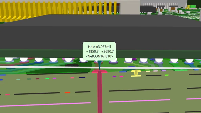
Steps
- Point the mouse at the place where you want to cut.
- Hold Delete and move the mouse to set the angle of the cut. The angle snaps in 45° steps; hold Shift as well for any angle. Release Delete.
- Hold Delete again and move the mouse to move the cut through the board.
- Press Escape to leave the cross-section and return to the full board view.
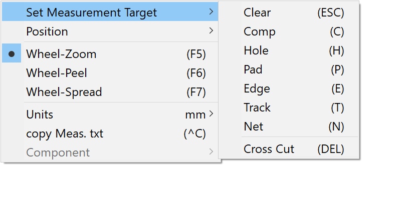
The first Delete sets the angle, the second moves the cut. The view updates in real time. Alternatively, right-click and choose Set Measurement Target → Cross-cut.
Tips
- Position over a via stack to verify all layers are correctly connected
- Use a diagonal cut to inspect angled traces
- Combine with Spread to see each layer's cross-section separately
- Use Orthogonal camera mode for a true 2D cross-section view
3.5 Colour presets and picker
Change how your board looks by applying colour presets or customising individual layer colours.
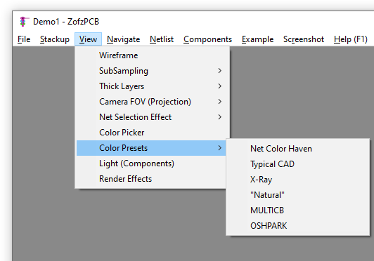
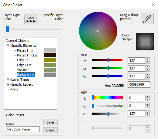
Colour presets
Go to View → Color Presets to select a built-in colour scheme.
Custom colour picker
- Go to View → Color Picker
- Select the layer you want to change
- Choose a colour: the change applies immediately
Colour settings are saved in your .camset and .zofzproj files.
3.6 Render effects and lighting
Fine-tune the 3D rendering appearance: wireframe, subsampling, thick layers, camera projection, and lighting.
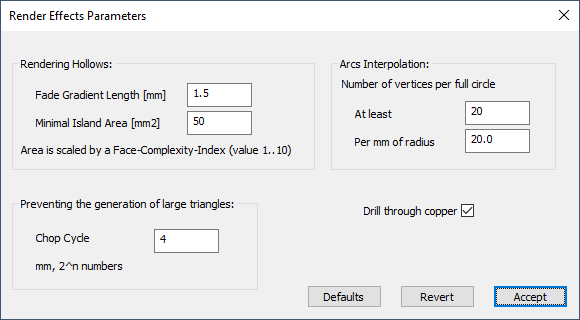
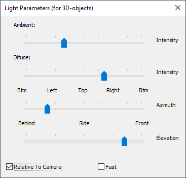
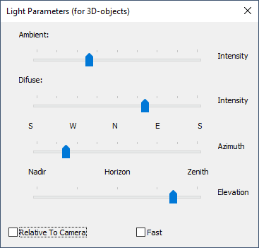
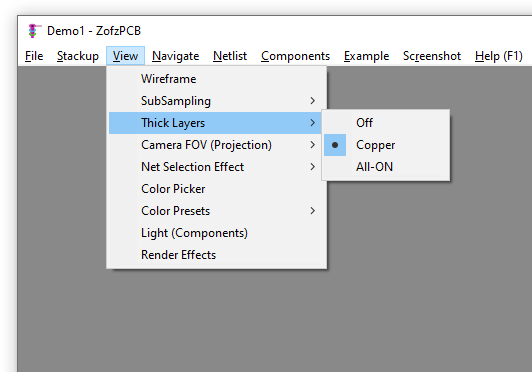
View menu options
| Option | Description |
|---|---|
| Wireframe | Show board as wireframe outline only |
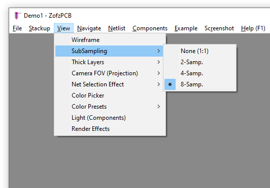
| SubSampling | Reduce render quality for better performance |
| Thick layers | Exaggerate layer thickness for clearer visualisation |
| Camera FOV | Adjust field of view |
| Net selection effects | Visual style for highlighted nets |
| Render effects | Post-processing effects on the 3D view |
| Light | Adjust light direction and intensity |
3.7 Screenshot and autopilot
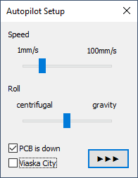
Capture high-resolution images of your board and use autopilot for automated rotation.
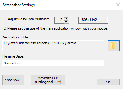
Screenshot
- Position the board as you want it
- Go to Screenshot in the menu bar
- Choose resolution and file format
- Select a save location and press Save
Screenshots capture the exact view: colour scheme, layer visibility, cross-sections, and any measurements or annotations currently visible.
Autopilot
Rotates the board automatically in a smooth continuous movement, useful for presentation sequences.
- Go to Autopilot in the menu bar
- Set rotation speed and axis
- Press Start / Stop
3.8 Show one layer alone
Click a layer's name (right of its checkbox) to show only that layer. Reset returns to the full board. In Spread mode, tick Single to peel layer by layer.
3.9 Mouse and keyboard
Hold Ctrl while turning the mouse wheel to zoom more slowly, Shift to zoom faster; this also works on the numeric keypad. All controls: Help → Mouse & Keyboard. A printable shortcut list (PDF) is in the Help menu.
3.10 Colors for realistic screenshots
In the color picker, the hex field takes 8 digits. For entries with an Opaque slider, put FF in front of the color; for entries without one (Plated H. In/Out, Edge Out, Background), put 00 in front. The colors we use for screenshots and cross-sections:
| Entry | Value |
|---|---|
| Copper | FFCB7B48 |
| Plated H. | 00D0D3D2 |
| Volume | FF6E7672 |
| Edge In | FF5F786C |
| Edge Out | 008FA69A |
| Background | 001B2B16 |
Components
Six articles covering 3D component models, from automatic generation to custom building.
Feature overview → Background: IPC-356 and 3D components →4.1 Auto 3D modeler
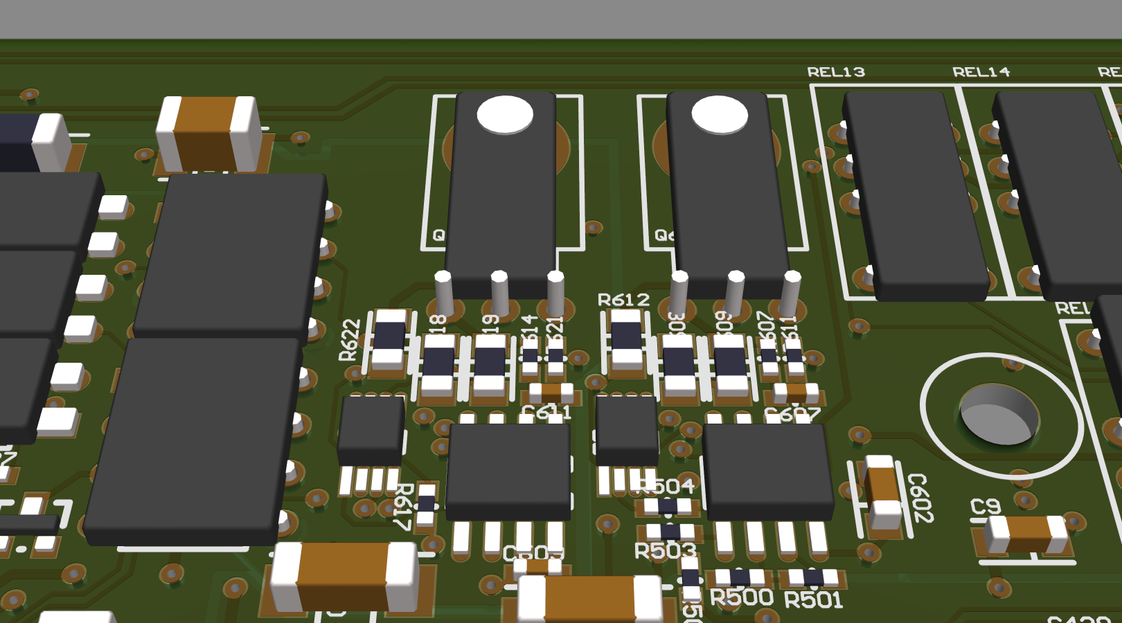
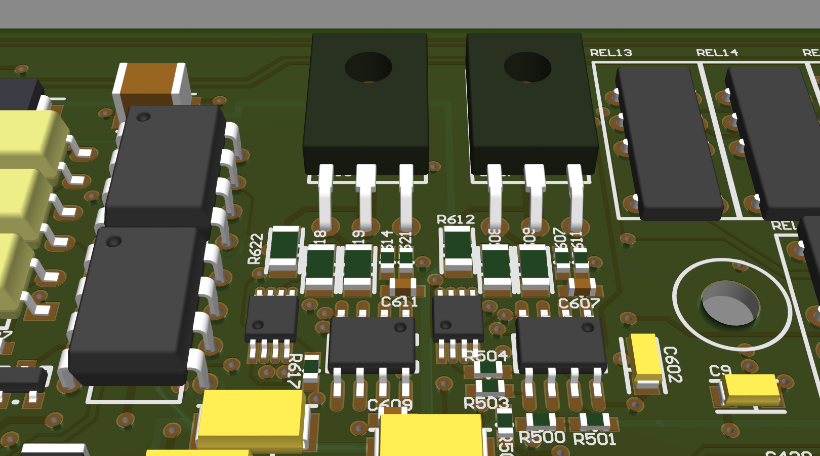
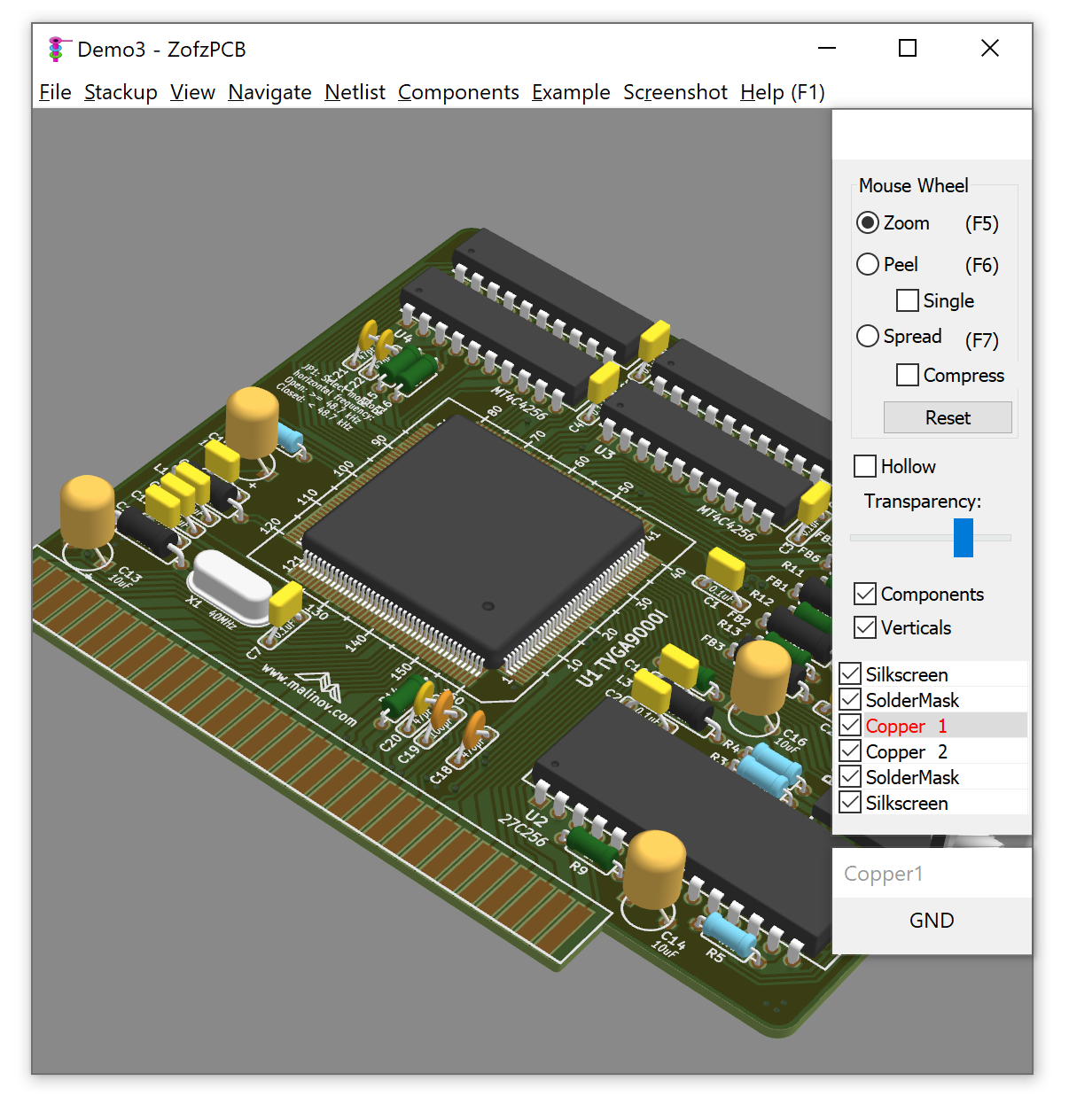
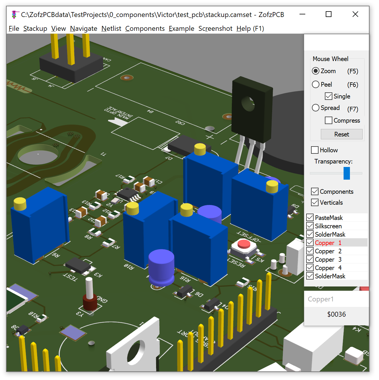
ZofzPCB automatically generates 3D component models from your BOM and PCB footprints, no library setup required.
How it works
The auto-modeler reads your BOM and IPC-356 netlist, then uses the PCB footprint geometry to generate a 3D model for each component.
| Variant | Description |
|---|---|
| Extruded | Free: simplified block-shaped models from the footprint outline |
| Realistic | Free: more detailed models with pin geometry and body shape |
Requirements
- A BOM file in CSV format must be loaded
- An IPC-356 netlist must be loaded
- Component references in the BOM must match those in the netlist
4.2 Component library
Browse and manage the 3D component model library for your project.
Accessing the library
- Go to Components in the menu bar
- The component list shows all components loaded from your BOM
- Components with 3D models show a model indicator
- Components without models are listed but appear as empty footprints in the 3D view
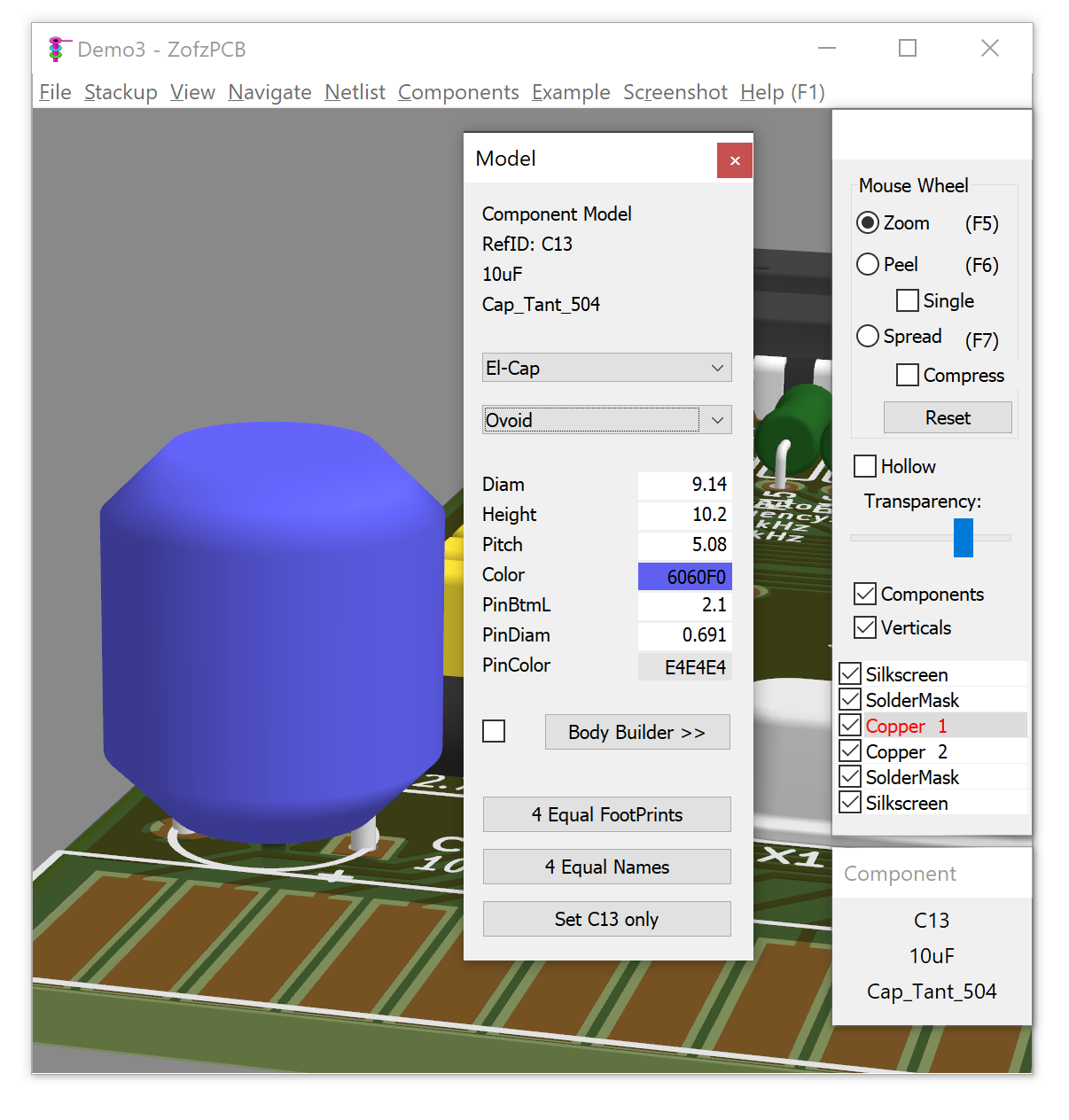
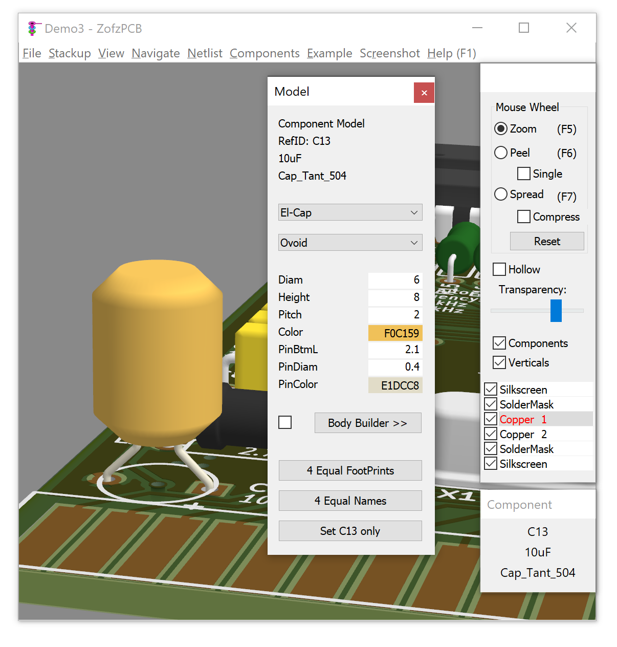
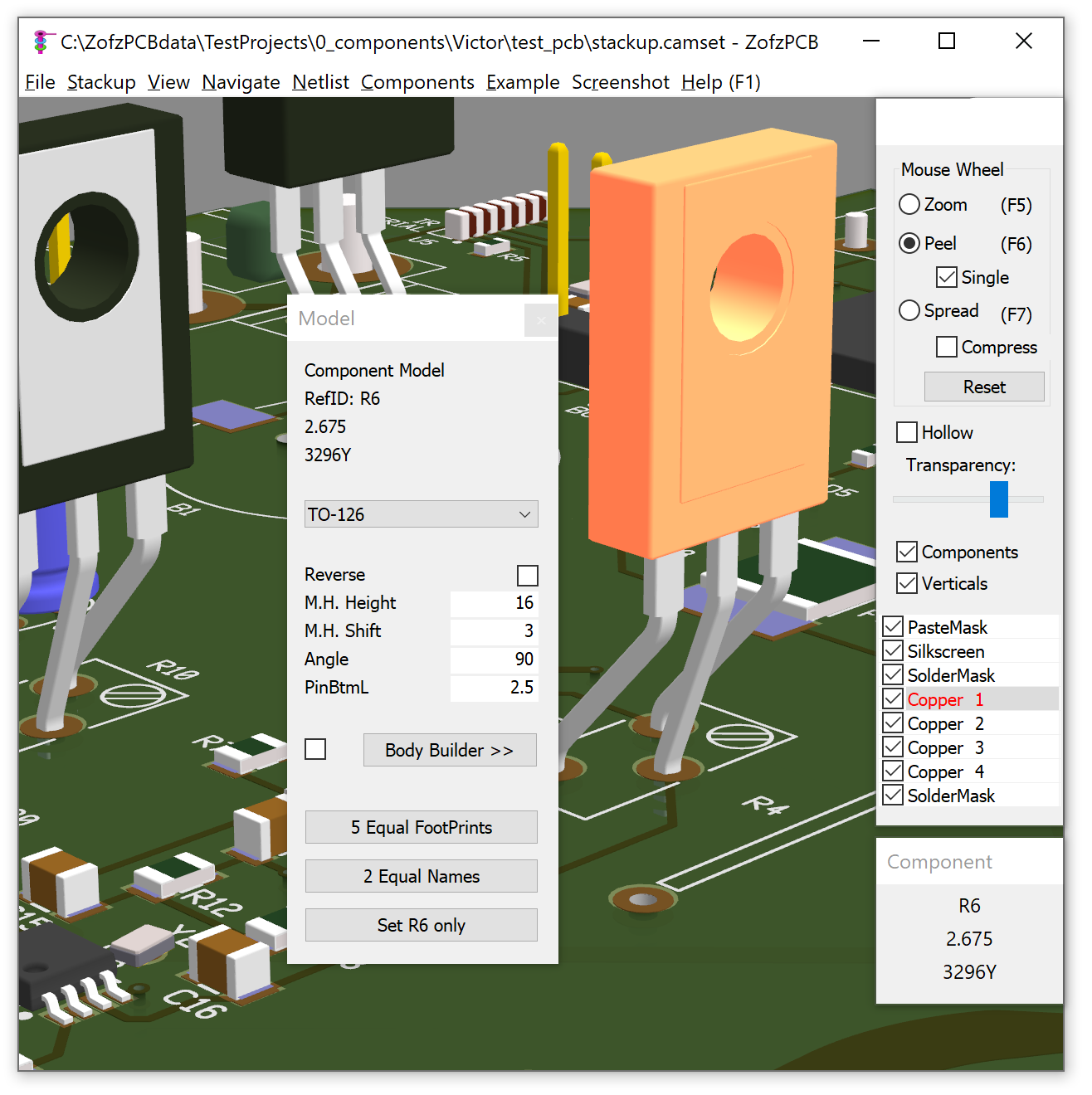
Adjusting component models
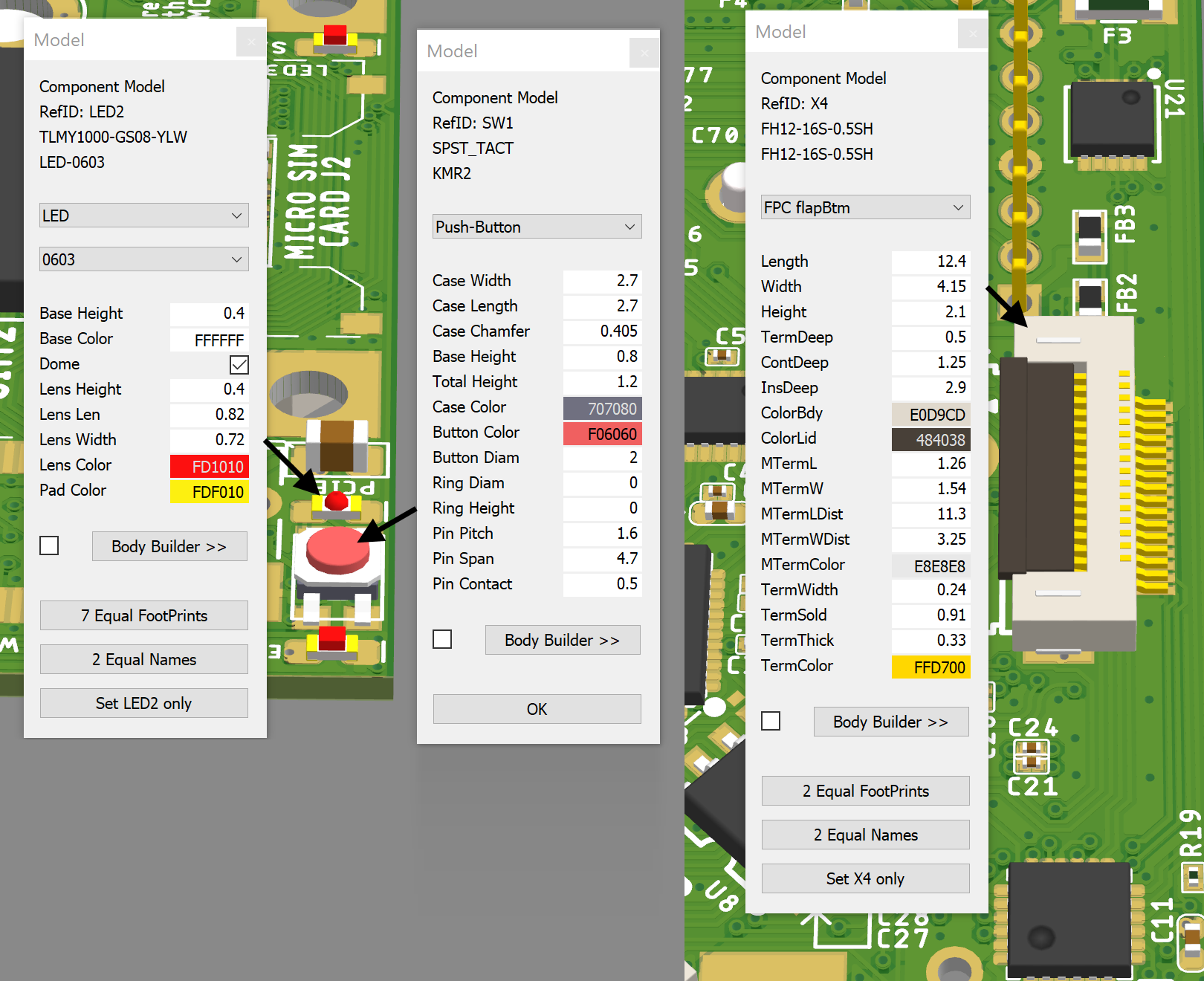
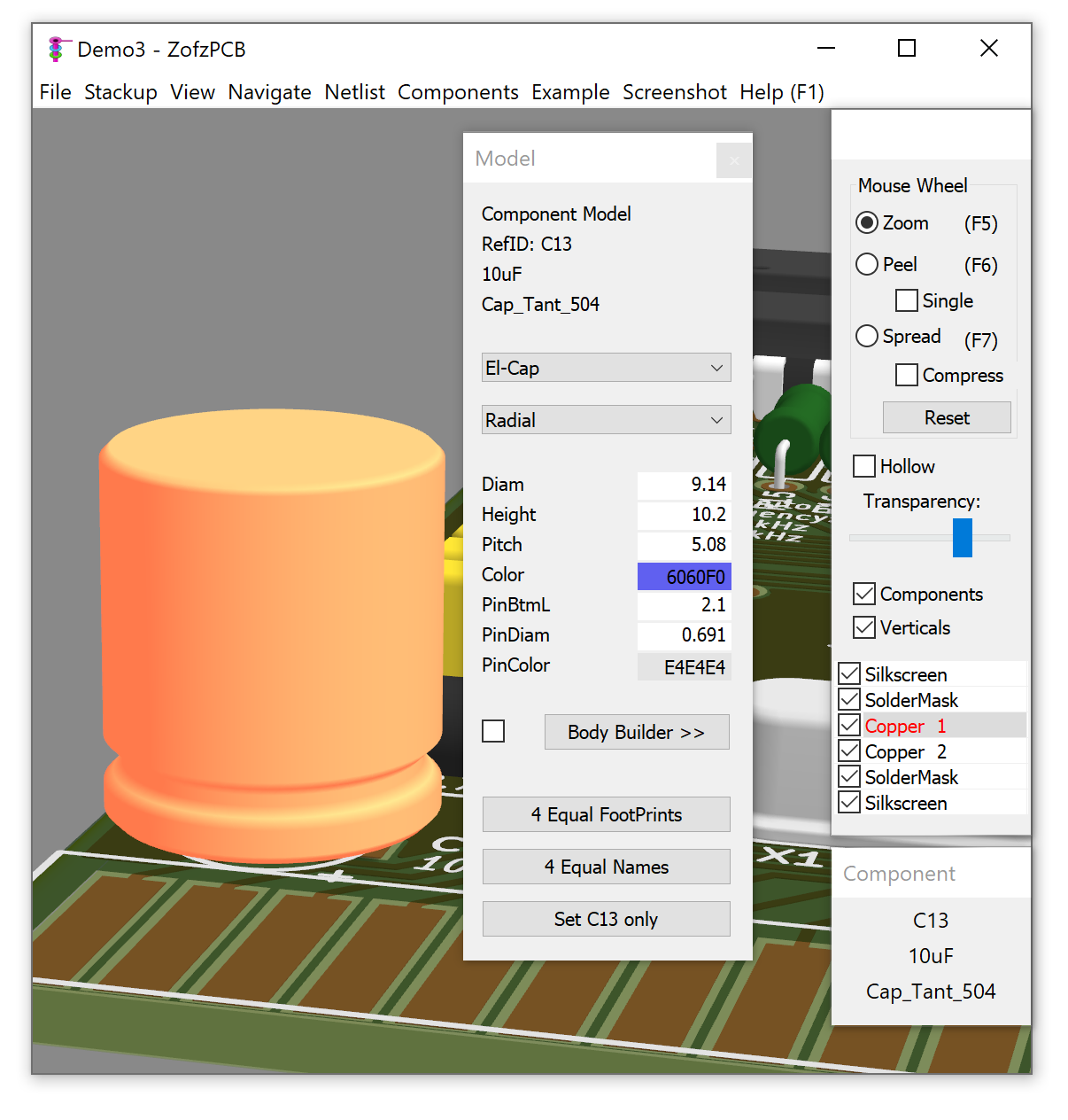
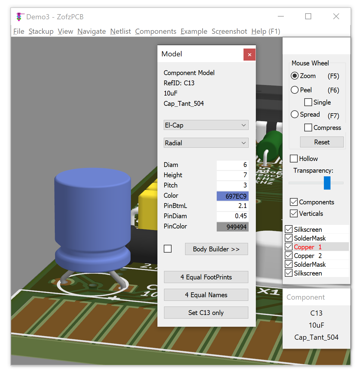
For each component you can:
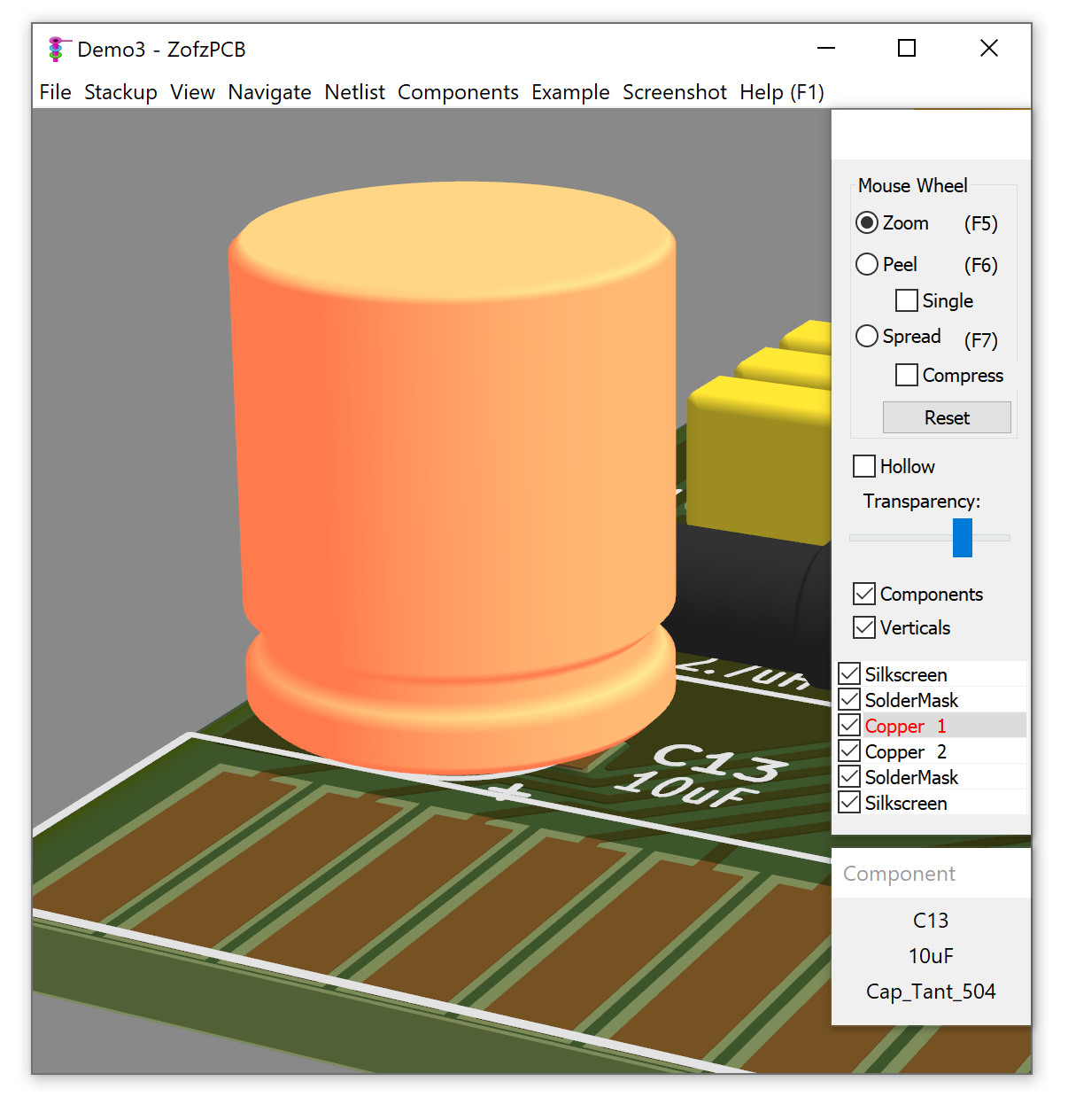
- Adjust model parameters: fine-tune the auto-generated model dimensions
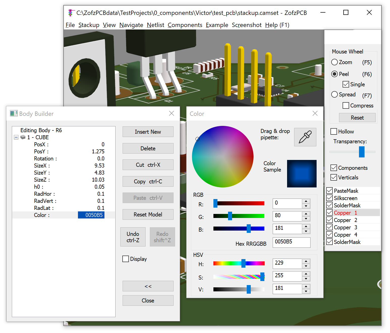
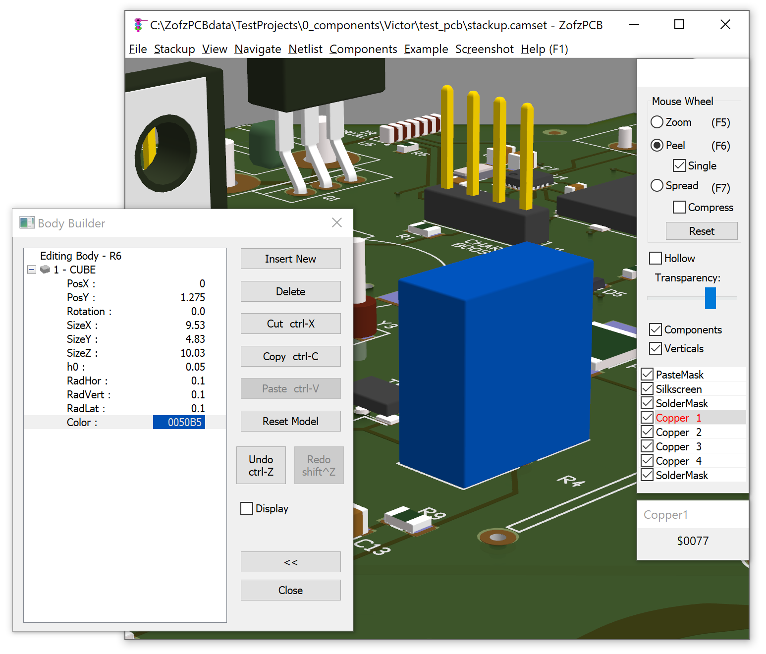
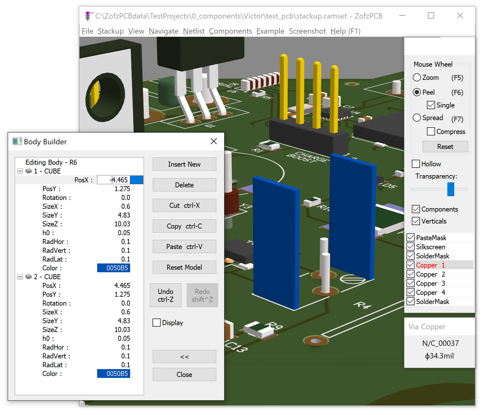
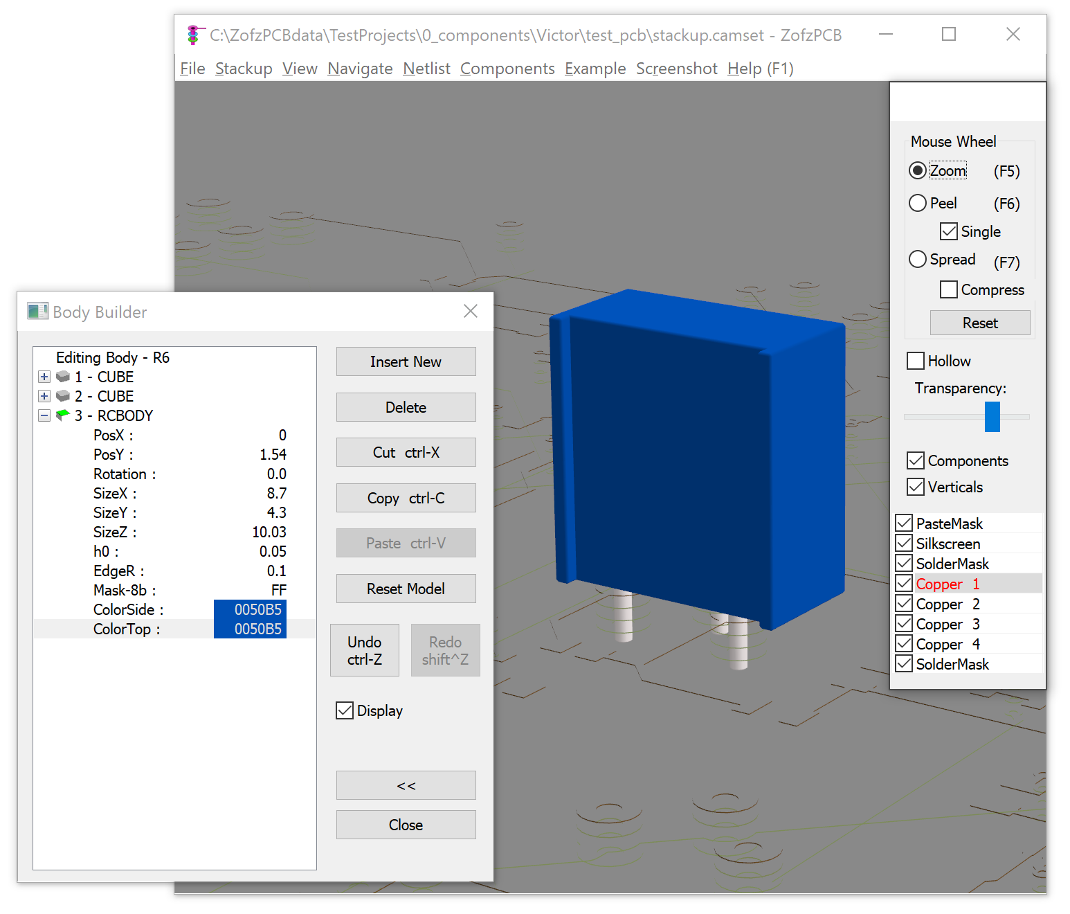
- Replace with Body Builder model: assign a custom model
- Override component height: set an exact height for the component body
Adjustments are saved in .camset and .zofzproj files and applied every time you reload the project.
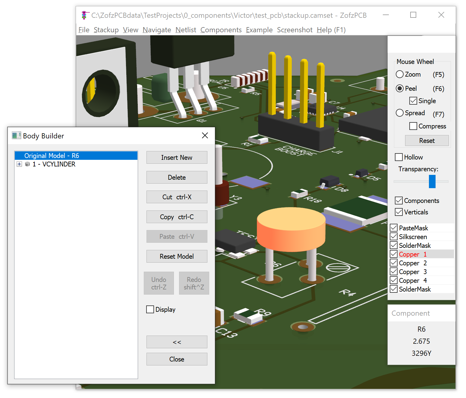
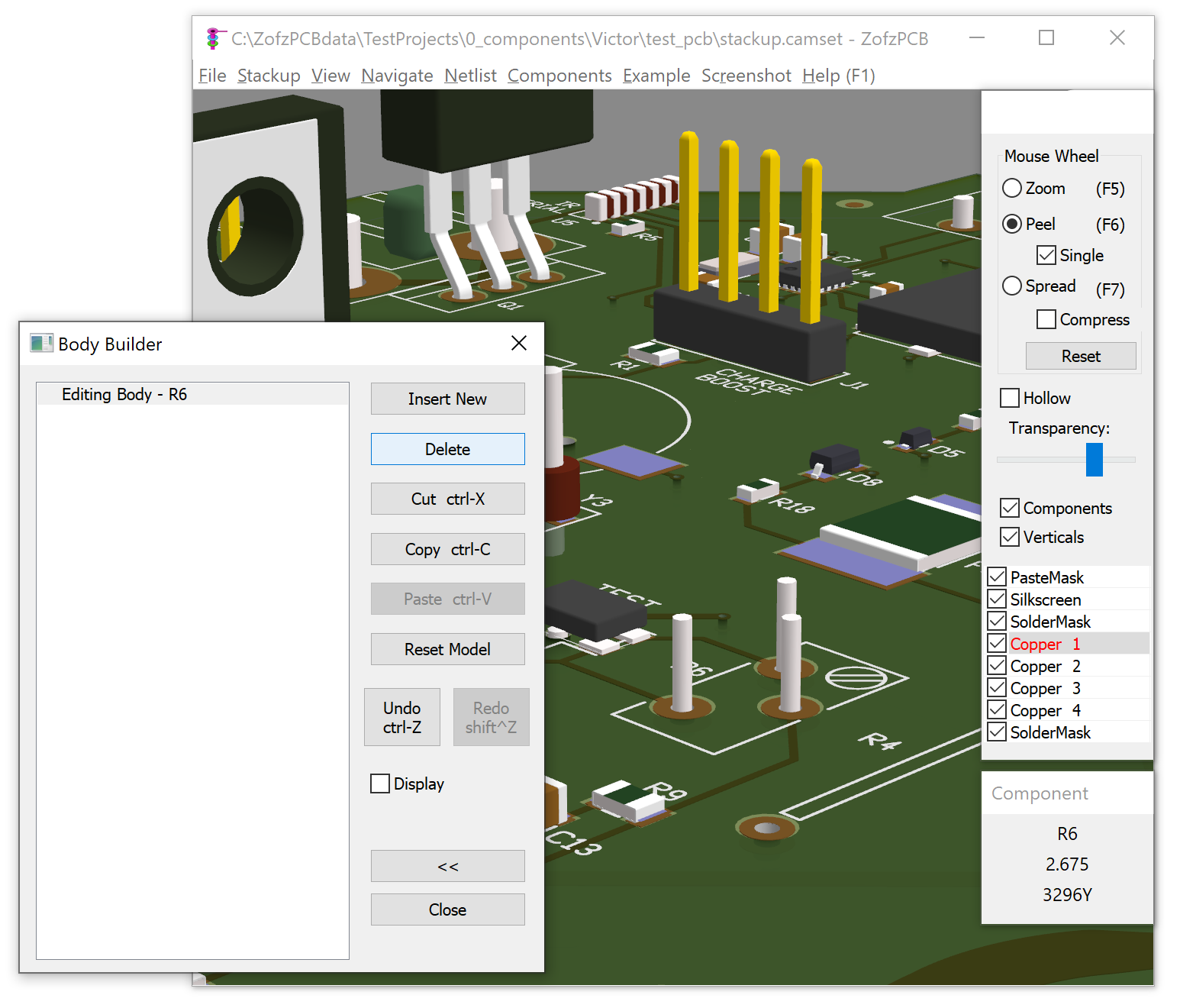
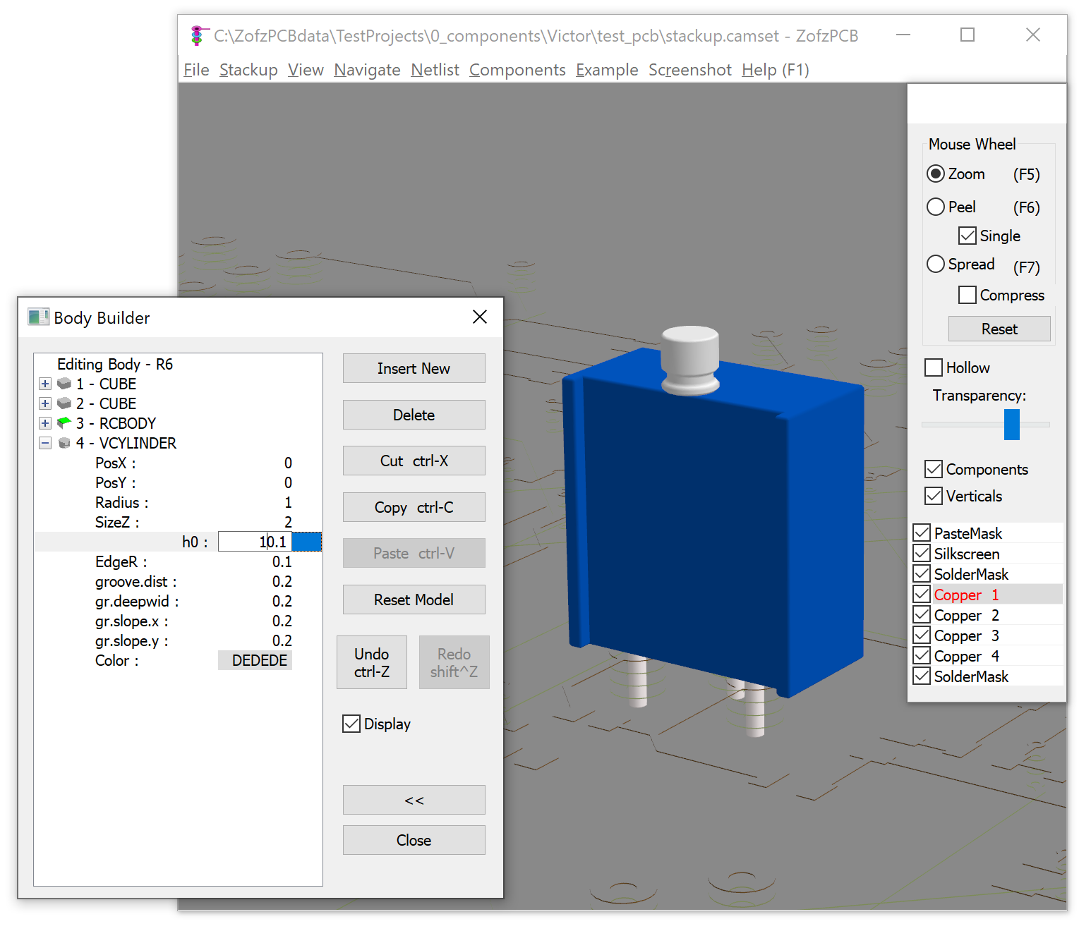
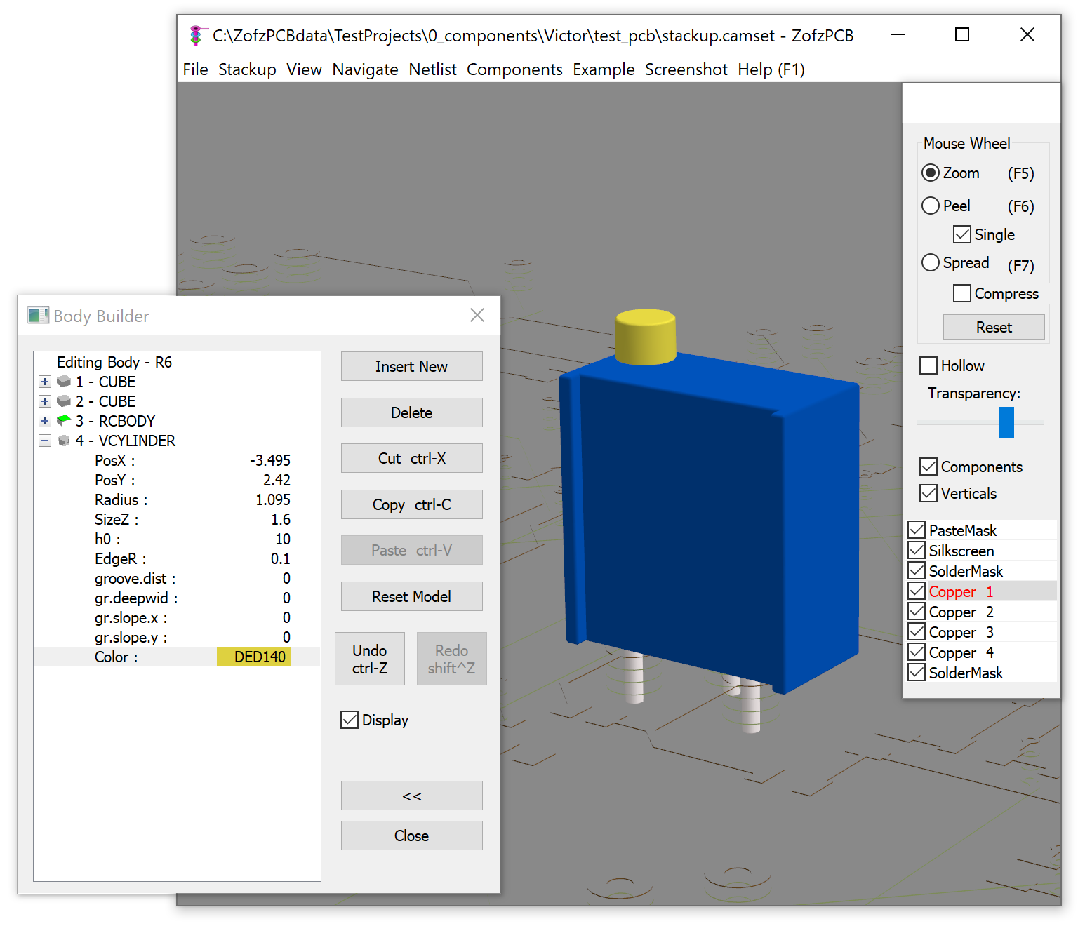
4.3 Body Builder
Create precise custom 3D models for components the auto-modeler cannot fully capture.
When to use this
- Exotic, custom, or proprietary components with non-standard geometries
- Exact 3D fidelity needed for mechanical interference checks or STEP export
- Component body shape critical for enclosure design or thermal simulation
How it works
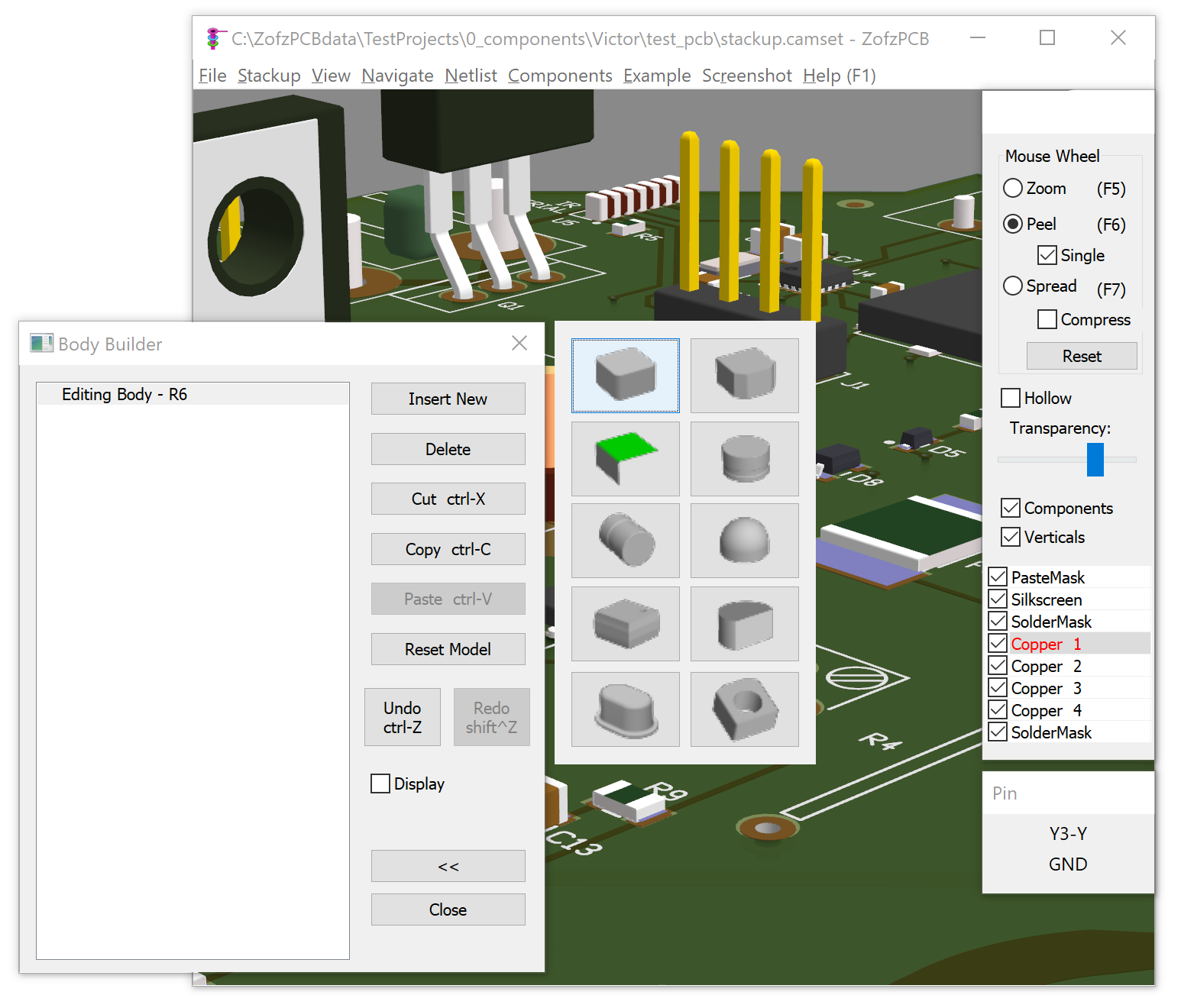
The Body Builder is a geometric editor where you define:
- Body dimensions: length, width, height
- Pin geometry: pin positions, sizes, and lead style
- Body shape: rectangular, cylindrical, or custom
Models are saved to your project's component library and reusable across all boards.
Steps
- Open the component library (Components menu)
- Select the component you want to model
- Click Body Builder
- Define the body dimensions
- Add pins and set their positions
- Press Save: the model is applied immediately
4.4 IPC-356 and BOM matching
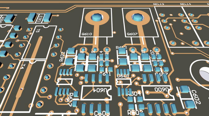
How ZofzPCB uses your netlist and BOM together to place component models, and what to do when matching fails.
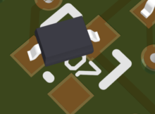
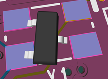
How matching works
ZofzPCB uses the IPC-356 netlist to identify component positions and pin connections, then matches these to BOM entries using the component reference designator (e.g. U1, C3, R12).
Common issue: truncated references
The IPC-356 format limits component reference names to 6 characters. Longer references (e.g. BTN_DOWN) are truncated (e.g. BTN_DN), causing a mismatch.
Solutions:
- Keep reference designators to 6 characters or fewer
- Check for duplicate truncated names: two references truncating to the same string will both fail
- Some CAD tools allow longer designators as a non-standard extension: check your export settings
Checking for errors
Go to Netlist → Errors to see components that could not be matched.
4.5 Change a component's model
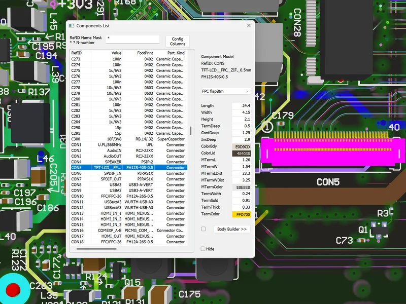
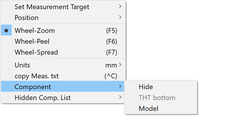
Right-click the component, then Component → Model. To change many parts at once, load a CSV BOM with your Gerbers. When ZofzPCB recognizes its columns, you can apply a model to all components with the same footprint or the same name. Check the result in the Components List (main menu: Components): it shows footprint and component name columns when the BOM was recognized.
Up and Down move between entries, and Enter finishes editing and jumps to the next line.4.6 Components missing in 3D
ZofzPCB detects components from the IPC-356 netlist. Pads that aren't connected to a net can be missing from the export, and then the component may not appear. Export an IPC-356 file that includes all pads, and a BOM with one reference designator per line. For an empty footprint, right-click it and pick a model from the Hidden Component List.
Inspecting your design
Eight articles covering design inspection: components, nets, vias, holes, and schematic crosscheck.
Feature overview →5.1 Browsing components
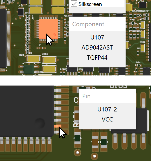
Find, highlight, and zoom to any component on your board instantly.
Steps
- Go to Components in the menu bar, or use the right panel component list
- Click any component: ZofzPCB highlights it and zooms to it across all layers simultaneously
- Or click the component directly on the board to select and zoom
Keyboard navigation
- N: jump to next component
- P: jump to previous component
What you can see per component
- 3D model in full context
- Pin positions and designators
- Component reference and value from the BOM
- Net assignments for each pin
5.2 Browsing nets and pins
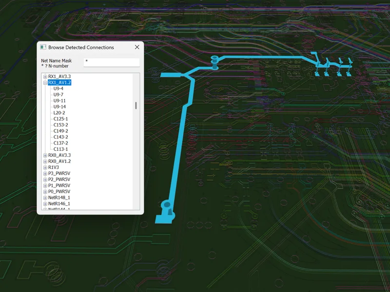
Trace any signal through your entire board in 3D, across all layers simultaneously.

Browsing nets
- Go to Netlist → Nets
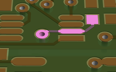
- Click any net: ZofzPCB highlights all copper belonging to that net across every layer
- Or click any trace, pad, or copper area on the board directly to highlight its net
Browsing pins
- Go to Netlist → Nodes PCB or Netlist → Nodes IPC
- Expand any net to see its pins
- Click any pin: ZofzPCB highlights and zooms to it
5.3 Browsing holes and vias
Inspect every hole and via on your board, including clearances, annular rings, and cut-through stack views.
Hole browser
- Go to Vias/Holes in the menu bar
- The hole browser lists every hole and via
- For each hole you see: hole diameter · pad diameter · annular ring width · clearance to adjacent copper · layer span
- Click any hole to highlight and zoom to it

Cut-through stack view
For any selected via, the hole browser shows a cross-section of the via stack, displaying all the copper layers it connects through.
5.4 Netlist error checking
Verify that the copper connections on your board match the IPC-356 netlist, and identify any discrepancies.
Steps
- Ensure your IPC-356 netlist is loaded
- Go to Netlist → Test to run the comparison
- Go to Netlist → Errors to view the results: Missing connections: nets in the IPC-356 with no copper connection; Extra connections: copper connections not in the IPC-356
- Click any error to highlight and zoom to the affected area
- Go to Netlist → Save Report to export the results
5.5 CrossCheck: schematic sync
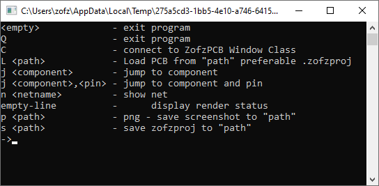
Navigate between your PCB in ZofzPCB and your schematic editor simultaneously.
CrossCheck modes
| Mode | Description |
|---|---|
| Disabled | Commands not sent; P and N keys act for selection |
| CPN: Comp Pad Net | C, P, N keys send crosscheck commands |
| C: cross-check | C key sends crosscheck; P and N keys act for selection |
| On Hover | Mouse hover triggers crosscheck |
Steps
- Set up the connection: see 9.2 Connecting to a schematic editor
- Go to Netlist → Cross Check and select your preferred mode
- Click or hover over a component or net: the schematic editor jumps to that element
5.6 Show only TH or SMD components
Components → Display only → TH or SMT. A black square in the Components checkbox in the right panel means a filter is active; click the checkbox to show all components again.
5.7 Netlist CSV export
File → Export → Netlist CSV writes one line per pad with these columns: component, pin, net, SMD/THT, side, x, y. The number of lines minus one is the total pad count.
5.8 Holes List
The Holes List groups all holes by type, diameter and layer span and shows how many there are. Select an entry to highlight those holes on the board; the status bar shows the count for the selected tool and for all holes. For each hole, the list shows annular ring and clearance per layer. Press H to jump between the board and the list.
Measuring
Four articles covering measurements: distances, clearances, net markers, and annotations.
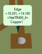
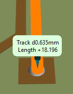
Feature overview →6.1 Distance measurements
Measure the distance between any two objects on your board in X, Y, Z, and XY.
Steps
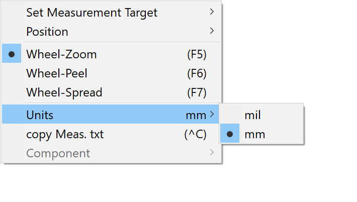
- Go to Measurements in the menu bar, or right-click → Measure
- Click the first object: a pad, hole, track edge, component body, or board edge
- Click the second object
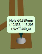
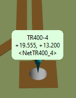
- ZofzPCB displays X, Y, Z and XY distances between the two points
Measurable objects
| Object | Examples |
|---|---|
| Pads | Pad centre, pad edge |
| Holes | Hole centre, hole edge |
| Tracks | Track centre, track edge |
| Component bodies | Body edge, body centre |
| Board edge | Any point on the outline |
Tips
- Use Orthogonal camera mode for 2D-style measurements
- Multiple measurements can be active simultaneously
- Measurements are saved in .camset and .zofzproj files
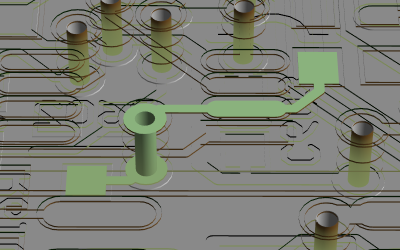
6.2 Net markers
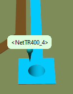
Add visual markers to nets on the board for annotation and inspection.
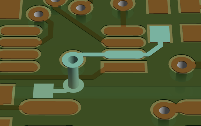
Steps
- Select a net by clicking on any copper belonging to it
- Go to Measurements → Net Marker
- A marker is placed on the selected net with the net name as its label
- Markers are visible in the 3D view and captured in screenshots
Managing markers
- Multiple net markers can be placed simultaneously
- Markers are saved in .camset and .zofzproj files
- Remove a marker by selecting it and pressing Delete
6.3 Text balloons
Add custom text annotations to the 3D view.
Steps
- Go to Measurements → Text Balloon
- Click the point on the board where you want the balloon to point
- Type your annotation text and press Enter
- The balloon appears with a leader line pointing to the selected location
Tips
- Text balloons are visible in screenshots
- Saved in .camset and .zofzproj files
- Drag a balloon to reposition it after placing
6.4 Orthogonal camera mode
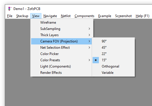
Switch to a true 1:1 scale 2D view for precise measurements and 2D-style inspection.
Steps
- Go to View → Camera FOV and select Orthogonal
- Navigate using the same mouse controls: pan with right button, zoom with scroll wheel
- All measurements in orthogonal mode are true 1:1 scale
- Return to perspective: View → Camera FOV → Perspective
When to use each mode
| Mode | Best for |
|---|---|
| Perspective | General 3D inspection, component visualisation |
| Orthogonal | Measurements, 2D-style review, printouts, cross-sections |
Compare revisions
Compare Designs plugin: Three articles covering revision comparison.
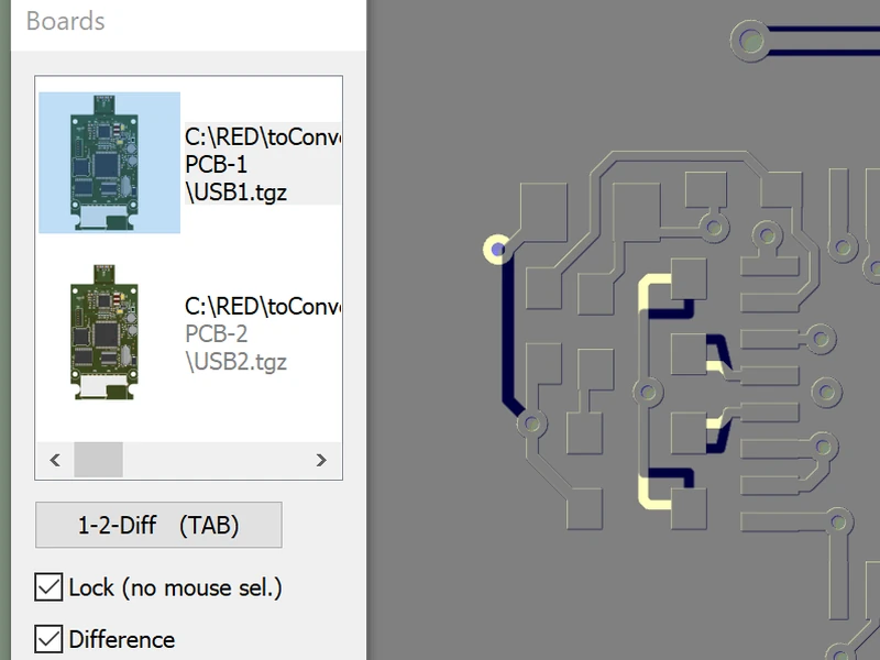
Feature overview →7.1 Loading two versions
Load two board revisions into ZofzPCB to prepare for comparison.
Steps
- Load your current board version as normal
- Go to File → Compare
- Select the second board version: Gerber set, ODB++, IPC-2581, or .zofzproj
- ZofzPCB loads both versions and overlays them in the 3D view with differences highlighted
Requirements
- Both boards must be the same design (same outline, same layer count)
- Both must be loaded from compatible file formats
- Best results when both versions share the same coordinate origin
7.2 Reading the diff overlay
Understand the colour-coded change indicators in the revision comparison view.
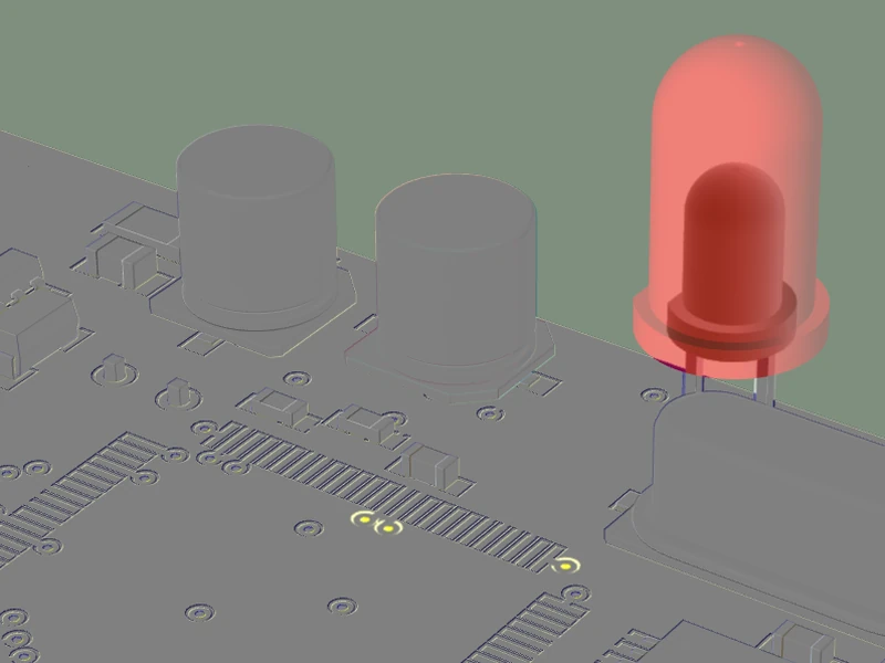
What the overlay shows
| Indicator | Meaning |
|---|---|
| Highlighted in copper colour | Element exists in the new version but not the old |
| Dimmed or removed | Element exists in the old version but not the new |
| Unchanged | Element is identical in both versions |
The comparison works across all layers simultaneously: a change on an inner copper layer is just as visible as one on the surface.
Navigating changes
- Use the layer panel to focus on one layer at a time
- Use cross-section to inspect changes on inner layers
- Zoom to any highlighted area to inspect in detail
7.3 Filtering changes
Focus on specific layers or types of changes in the revision comparison view.
Filtering by layer
Use the layer panel to hide all layers except the one you want to review.
Filtering by change type
Use the compare controls to show:
- Additions only: elements in the new version but not the old
- Removals only: elements in the old version but not the new
- Both: all changes
Tips
- Combine layer filtering with cross-section to inspect inner layer changes in isolation
- Use the component browser to check if specific components changed position or orientation
Export and share
STEP export and View-Only Mode: Three articles covering how to get your board model out of ZofzPCB.
Feature overview →8.1 STEP file exportSTEP Export plugin
Export a complete 3D model of your board for mechanical CAD, simulation, or documentation.
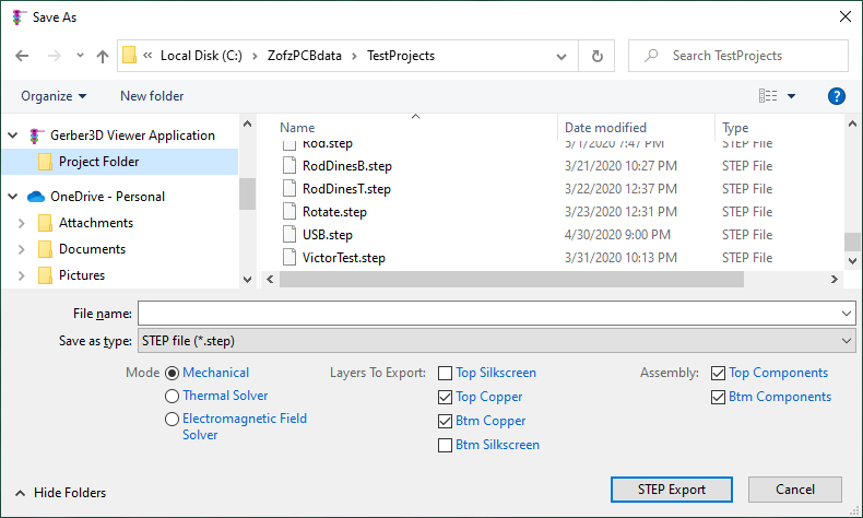
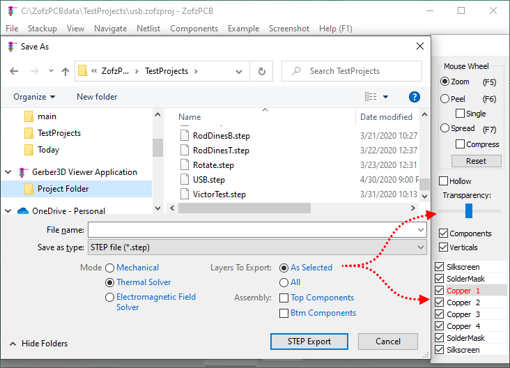
What the STEP file includes
- Board outline and PCB shape
- All copper layers
- Every mounted component as a structured assembly element
- Board thickness and stackup geometry
Steps
- Ensure your stackup dimensions are correctly entered, see 2.2 Layer types and thickness
- Ensure all components have 3D models, see 4.1 Auto 3D modeler and 4.3 Body Builder
- Go to File → Export STEP
- Choose a filename and save location
- Press Export
Compatible applications
SolidWorks · CATIA · Fusion 360 · FreeCAD · Any mechanical CAD or simulation tool that supports STEP (ISO 10303)
8.2 View-only sharing
Share an interactive 3D view of your board with colleagues or clients, no ZofzPCB installation required.
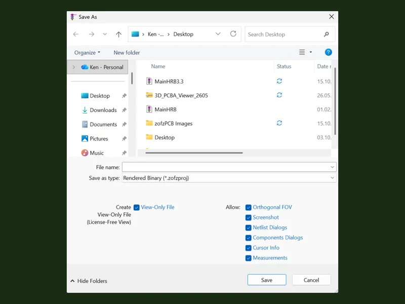
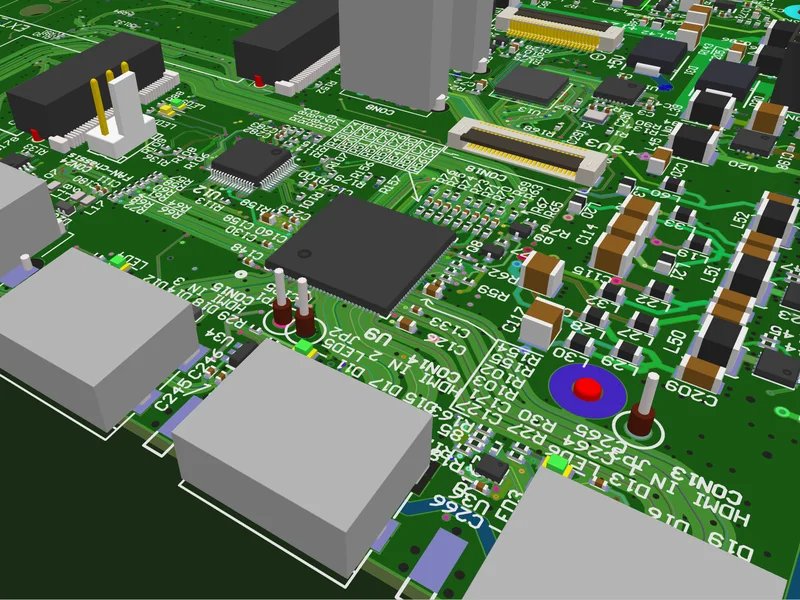
What recipients can do: rotate, zoom, pan, inspect from any angle
What recipients cannot do: modify, export, or access source files
Method 1: Save as view-only .zofzproj
- Go to File → Save As
- Select .zofzproj as the file type
- Check the View-Only Mode option before saving
- Share the .zofzproj file: recipients open it in the free version of ZofzPCB
Method 2: pcbmodel.com gallery
Share your board publicly via the PCB Model gallery at pcbmodel.com.
8.3 Screenshot export
Save a high-resolution image of your current 3D view.
Steps
- Set up the view: angle, zoom, layer visibility, colour scheme, annotations
- Go to Screenshot in the menu bar
- Select output resolution and file format
- Choose a save location and press Save
Tips
- Screenshots capture all visible annotations: measurements, net markers, text balloons
- Use a high resolution for print-quality output
- Use Orthogonal camera mode for a clean 2D-style top-down view
CrossCheck: programmatic interface
Two articles covering ZofzPCB's programmatic interface for connecting to external tools.
9.1 What is CrossCheck?
CrossCheck is ZofzPCB's programmatic interface for connecting to external tools, primarily schematic editors.
Overview
CrossCheck allows ZofzPCB to communicate in real time with a schematic editor running alongside it. When you click a component or net in ZofzPCB, CrossCheck sends a command to the schematic editor to navigate to that same element, and vice versa.
Use cases
- Design review: click a component in ZofzPCB and jump to it in the schematic instantly
- Error tracing: found a net error? Jump to the schematic to find the source
- Cross-discipline review: share a live review session between PCB and schematic designers
How it works technically
ZofzPCB exposes a command interface that external tools can connect to. CrossCheck sends component, pad, and net identifiers to the connected tool, which then navigates accordingly. The keyboard and mouse control mapping is configurable.
9.2 Connecting to a schematic editor
Set up a live connection between ZofzPCB and your schematic editor.
Supported tools
CrossCheck has been tested and documented with OrCad Capture. Other schematic editors that support external command interfaces may also work.
For a live demo: zofzpcb.com/Cross-Check
Steps (OrCad Capture)
- Open both ZofzPCB and OrCad Capture with the same design loaded in each
- In ZofzPCB, go to Netlist → Cross Check
- Select your preferred CrossCheck mode: CPN: Comp Pad Net: C, P, N keys send crosscheck commands; C: cross-check: only the C key sends commands; On Hover: mouse hover triggers commands automatically
- In OrCad, configure the external command receiver to accept ZofzPCB's commands
- Click a component in ZofzPCB: OrCad should navigate to the same component
Configuring key mapping
Keys and mouse functions used for CrossCheck commands can be customised in the CrossCheck submenu.
Troubleshooting
Reference
Five reference articles covering shortcuts, file formats, system requirements, performance, and bug reporting.
10.1 Keyboard and mouse shortcuts
Navigation
| Action | Control |
|---|---|
| Rotate | Left mouse button + drag |
| Pan | Right mouse button + drag |
| Zoom | Scroll wheel |
| Reset view | Spacebar |
| Next component | N |
| Previous component | P |
Layer control
| Action | Key |
|---|---|
| Peel top layer | F6 |
| Spread / compress layers | F7 |
| Set cross-section angle (45° steps) | Hold Delete + move mouse |
| Set any angle | Hold Shift + Delete + move mouse |
| Move the cut through the board | Hold Delete again + move mouse |
| Leave cross-section | Escape |
Selection
| Action | Control |
|---|---|
| Select object | Left click |
| Highlight net | Left click on copper |
| Context menu | Right click |
CrossCheck (when enabled)
| Action | Key |
|---|---|
| CrossCheck component | C (in CPN or C mode) |
| CrossCheck pad | P (in CPN mode) |
| CrossCheck net | N (in CPN mode) |
10.2 Supported file formats
Input formats
| Format | Type | Notes |
|---|---|---|
| Gerber RS-274X | Layer images | Industry standard: most common |
| Gerber X2 | Layer images | Extended format with layer attributes |
| Excellon | Drill files | Standard drill format |
| Gerber (drill) | Drill files | Preferred over Excellon for accuracy |
| IPC-356 | Netlist | For component placement and net checking |
| BOM (CSV) | Bill of materials | For component models |
| ODB++ | Complete design | Single packed format |
| IPC-2581 | Complete design | Single XML format: recommended |
| ZIP | Archive | Gerber sets and IPC-2581 loadable from ZIP |
Output formats
| Format | Type | Notes |
|---|---|---|
| .zofzproj | Rendered project | Complete saved board with all settings |
| .camset | Configuration | Stackup and settings only |
| STEP | 3D model | For mechanical CAD: STEP Export plugin |
| PNG / JPG | Screenshot | Static image export |
10.3 System requirements
Minimum requirements
| Component | Minimum |
|---|---|
| Operating system | Windows 10 (64-bit) |
| Runtime | Microsoft VC++ Runtime (download link on the download page) |
| DirectX | DirectX 11 |
| Input | Scroll wheel mouse (required) |
| GPU | Integrated GPU of a modern PC or laptop |
| RAM | 4 GB |
Recommended for large boards
| Component | Recommended |
|---|---|
| Operating system | Windows 11 (64-bit) |
| GPU | Dedicated gaming-level GPU |
| RAM | 8 GB or more |
GPU notes
- Small to medium boards: integrated GPU sufficient
- Large, complex boards: dedicated GPU strongly recommended
- DirectX 11 required: if ZofzPCB does not start, update your graphics drivers
10.4 Performance and GPU
Tips for improving 3D rendering speed, especially for large or complex boards.
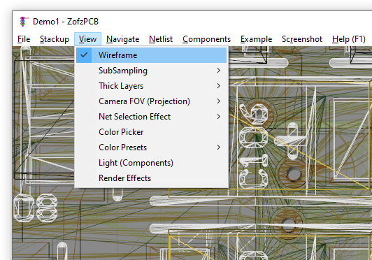
Steps to improve performance
- Lower SubSampling: go to View → SubSampling and reduce the level. Biggest single impact on performance
- Turn off unused layers: use the right panel to hide layers you don't need
- Toggle off components: uncheck Components in the right panel if 3D models aren't needed
- Close other GPU-intensive applications running in the background
- Check GPU assignment (laptops): make sure Windows is using the dedicated GPU for ZofzPCB: go to Windows Settings → Display → Graphics, find ZofzPCB and set to High performance
- Update graphics drivers: outdated drivers are a common cause of performance issues
Hardware recommendations
| Board size | GPU recommendation |
|---|---|
| Small to medium | Integrated GPU sufficient |
| Large / many layers | Dedicated gaming GPU recommended |
10.5 Reporting bugs
How to report issues, unexpected behaviour, or crashes to the ZofzPCB team.
Option 1: Contact form
Use the contact form. Include:
- ZofzPCB version number (shown in the title bar)
- Description of what happened and what you expected
- Steps to reproduce the issue
- Relevant files (Gerber set, .camset, or .zofzproj) if file-specific
- A screenshot if it helps
Option 2: Email
Contact the team directly at zofz@zofzpcb.com
Helpful information to include
ZofzPCB version · Windows version · GPU model · Description and reproduction steps · Example files if relevant