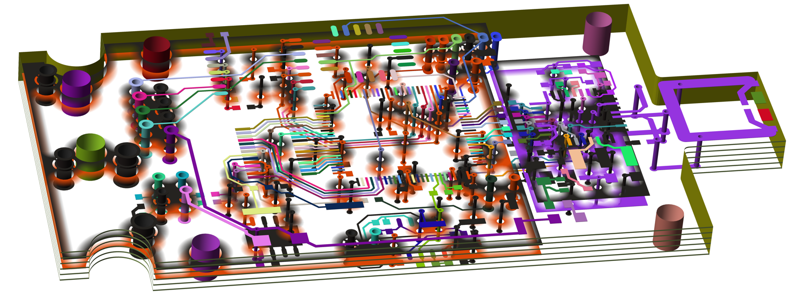

3D Viewer
Pros and Cons of 3D visualization. Why is this worthwhile?
At ZofzPCB, we understand the importance of visualizing circuit board designs in the most accurate and comprehensive way possible. That's why we've developed our 3D Viewer, a powerful tool that offers a number of benefits for circuit board designers. However, as with any tool, there are also some downsides to consider. In this article, we'll explore the pros and cons of using a 3D viewer for circuit board design visualization, and explain why it's worthwhile to use it.
Pros
- A Different View: One of the main advantages of using a 3D viewer is that it allows users to see a different perspective of the design, providing a more comprehensive understanding of the circuit board. This can help users find aspects of the design that may have been hidden in a 2D view.
- Stackup is an Integral Part of the View: The 3D Viewer on ZofzPCB website integrates the stackup feature, making it easy to understand the overall structure of the board, from the different layers to the components placement.
- Color as the Missing Z-Dimension: In 2D viewer, the third dimension is often shown by adding artificial colors to layers. In the 3D Viewer, color is free to use, it can be natural or artificial, and can also be used to show netlist connections. This provides more flexibility and can enhance the understanding of the layout and placement of components.
- 3D Game Mechanics and Fantastic Imaginary: The 3D Viewer allows users to have an immersive experience of the board, making it possible to have a better understanding of how the board works, and how the components interact, this can be a fun way to explore the board.
- Components Make Sense: With the 3D Viewer, users can see the board's components in a more realistic way, which helps to understand how the components are placed and how they interact with other components.
Cons
- Battery Usage: The use of GPU will add speed to the display, but it also increases the device's battery usage, which can be an issue for users working on the go or with limited power sources.
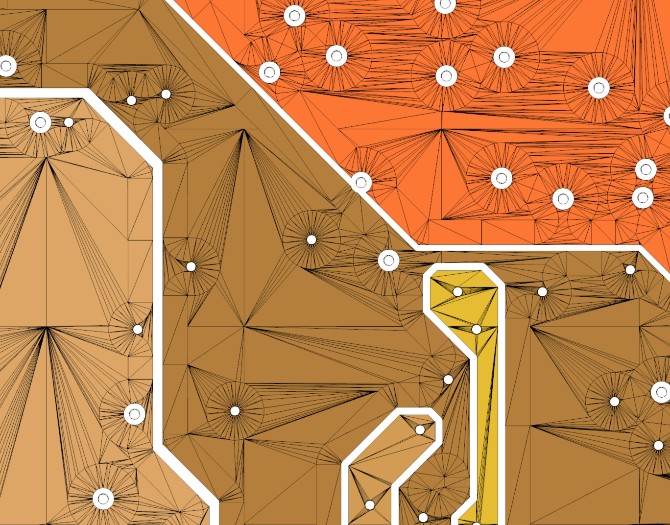
- Flattening and Triangulation (Extensive Load Time): The process of flattening and triangulation can lead to extensive load times, which can be frustrating for users.
- Entering Stackup Dimensions and Order (Sometimes Annoying): The process of entering the stackup dimensions and order can sometimes be annoying, but it is necessary to correctly visualize the board.
- New Approach - May Require You to Move Out of Your Comfort Zone: The 3D Viewer may require users to move out of their comfort zone, as it's a new approach to circuit board visualization.
In conclusion, the 3D Viewer on the ZofzPCB website is a powerful tool that offers many benefits for circuit board design visualization. While there are some downsides to consider, the benefits of the 3D viewer outweigh the cons, making it a valuable tool for designers looking to improve their circuit board visualization and to find issues or mistakes on the board. The 3D Viewer is a fun and interactive way to explore the board, making it a worthwhile tool for anyone working on circuit board design. Users should be aware that the use of the 3D Viewer may increase battery usage and plan accordingly. The flexibility of color usage in the 3D Viewer can be very helpful for understanding the board layout, and showing netlist connections.
Rendering
ZofzPCB uses a GPU (Graphics Processing Unit) via Direct3D to display the image. The drawn/painted layer contains a lot of overlapped objects. Another example is a track in a plane. First, a part of the plane is cleared, and other elements are drawn in the resulting hole. All this higher-level construct must be converted to optimal positive mesh. The result is that even a complicated PCB can be displayed by moderate GPU, usually at 60fps.
A drawback of the flattening stage and triangulation is the time it takes before passing the mesh to the GPU.

The 3D rendering is nicely described in the YouTube video:
How do Video Game Graphics Work?".
ZofzPCB uses mechanisms described up to 17:20 out of 21 minutes of this video.
There is still a lot to do for future development by applying textures (overlapping bitmaps), especially
for the components. The above video does not explain the texturing, btw.
Another development direction would be better lighting. At the moment, ZofzPCB uses Ambient and Diffuse Lighting.
Adding the Specular Lighting could produce a better view.
Animation and Navigation
The rendering speed allows animating the displayed components, creating unique impressions of rotation, movement, spreading, and stripping layers of the PCB.
The approach lets you keep the frame of reference - it is clear where you are, what had happened to create a particular view.
Please see the video below, showing the navigation possibilities.
Please see the video below, showing the animated selection of layers.